| Transmission Electron Microscopes |
| STEM Nion HERMES 200 kV monochromated and aberration-corrected |
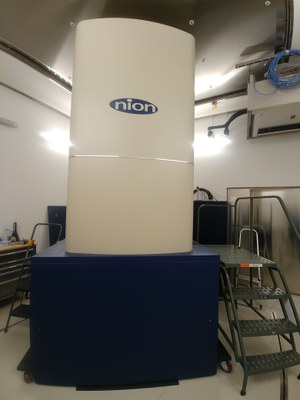 |
- 200 kV, field emission gun
- monochromated (energy resolution < 6 meV)
- aberration-corrected (probe size at 200 kV < 0.07 nm)
- side entry stage (double-tilt cryo holder with electrical contacts, etc.)
- direct detector for EELS and zero-loss filtered diffraction (Dectris)
- sample in ultra-high vacuum
|
| |
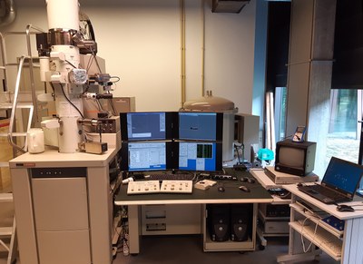
| TEM/STEM JEOL JEM2200FS |
(click on image to enlarge) |
- 200 kV, field emission gun
-
UHR pole piece
-
1k slow-scan CCD camera (Gatan)
-
ASTAR system (NanoMegas) including Beam precession unit, SNBD system, ACOM software
-
BF STEM detector
-
HAADF STEM detector
-
Electron biprism
-
Digiscan system (Gatan)
-
In-column energy filter
-
LN2 free energy dispersive X-ray SD detector (Bruker)
|
| |
| TEM/STEM FEI TITAN 80-300 Image Cs-corrected |
Cryo-TEM JEOL JEM2100 cryo |
Access via
Joint Laboratory for Electron Microscopy Adlershof (JEMA)
in cooperation with
Leibniz Institute for Crystal Growth
|
Access via
Joint Laboratory for Structural Research (JLSR)
in cooperation with
Helmholtz Centre Berlin and Technical University Berlin
|
|
|
|
- 300 kV, field emission gun
-
CEOS image Cs-corrector
-
2k x 2k camera
-
|
|
| |
| Scanning Electron Microscope |
| Zeiss GeminiSEM 500 |
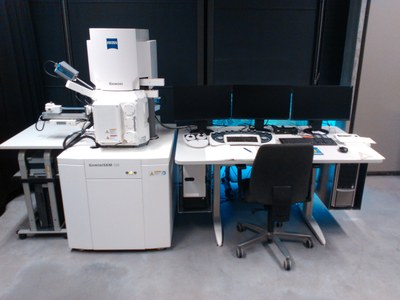 |
- NanoVP Option
- In-lens SE detector
- In-lens EsB detector
- BSE 4-Quandrant detector
- STEM detector
- Bruker XFlash 6|30 EDX system
- Raith ELPHY Quantum Lithography system
- Custom stages for 4D-STEM
|
| |
| TEM Sample Preparation |
|
Goal: Fabrication of samples having only some nanometer thickness with as few preparation artifacts as possible.
|
| |
| Instrumentation for preparation of hybrid inorganic/organic materials systems and soft matter. |
|
Ultramicrotome cutting
|
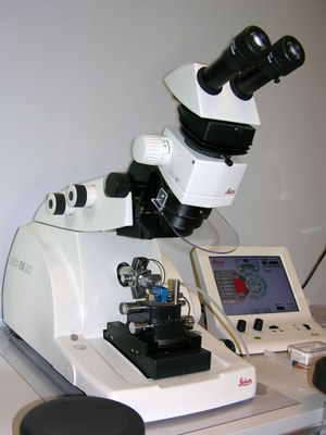 |
EM Ultracut 7 (Leica) |
| |
| Instrumentation for conventional TEM preparation of inorganic semiconductors. |
|
Formatting
|
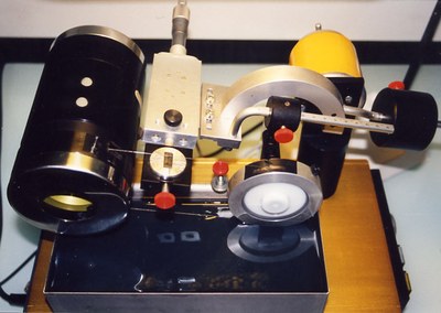 |
Diamond wire saw (Dwell) |
|
Polishing
|
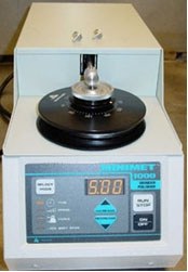 |
Minimet polishing machine (Bühler) |
|
Dimpling
|
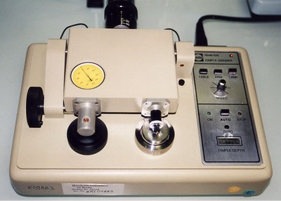 |
Dimple grinder (Gatan) |
|
Ion Milling
|
|
Rapid etching system RES101 (Baltec)
|
|
Ion Milling
|
|
Rapid etching system RES010 (Baltec)
|
|
Ion Milling
|
|
Rapid etching system RES010 (Baltec) - Low Voltage
|
|
Ion Milling
|
|
Precision ion polishing system (PIPS) (Gatan)
|
| |
| Optical Microscope |
| |
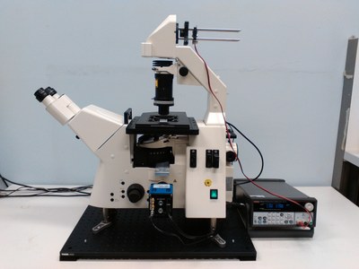
| Zeiss Axiovert 200M |
 |